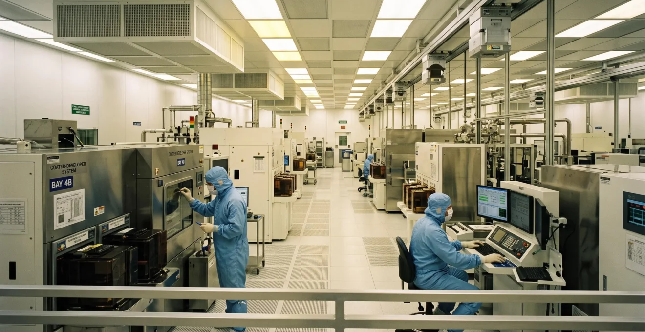
Run a 300mm fab and you already know the answer to the question this comparison seems to pose: you don’t choose between KLA, ASML and Applied Materials. You use all three, every day, on every wafer. The “vs” framing that drives most searches around the semiconductor equipment market is operationally misleading — and understanding why changes how you budget, negotiate, and manage your installed base.
Réponse directe :
KLA, ASML and Applied Materials are not direct competitors. ASML dominates EUV and advanced lithography, Applied Materials leads across deposition and etch, and KLA leads process control and metrology. A modern fab depends on all three simultaneously — the real question is how to manage that multi-vendor ecosystem, including maintenance and spare parts strategy.
The core insight. Comparing the big three of wafer fabrication equipment (WFE) by size or “who wins” misses the point. Each holds a distinct, hard-to-substitute position: lithography for ASML, deposition/etch for Applied Materials, process control for KLA. That complementarity shapes every fab’s equipment park — and its lifecycle and aftermarket exposure.
- The semiconductor equipment landscape: a record-scale ecosystem
- ASML: the lithography monopoly reshaping chip economics
- Applied Materials: breadth across deposition and etch
- Where does KLA’s process control fit in the value chain?
- How do their market positions compare?
- What operational factors matter beyond equipment performance?
The semiconductor equipment landscape: a record-scale ecosystem
The wafer fabrication equipment market is not just large — it is still expanding. According to SEMI’s global equipment sales forecast, total semiconductor equipment sales are projected to reach a record 123 billion. SEMI this momentum primarily to demand in advanced logic and memory — DRAM and HBM capacity tied to AI workloads.
Within that ecosystem, ASML, Applied Materials and KLA consistently rank among the largest WFE suppliers by revenue. Yet their combined footprint tells only half the story. What makes these three the natural subjects of any serious comparison is not their aggregate market share — it is the fact that they dominate three technologically distinct and largely non-substitutable segments.
The operational reality confirms it. A 300mm fab producing advanced automotive or IoT chips cannot run on a single vendor: ASML lithography systems define the patterns, Applied Materials deposition and etch tools build the layers, and KLA systems inspect and measure at every critical step. Remove any one of the three, and the line stops. That is why the more useful framing is not “who to choose” but “how to manage a structural dependence on all three” — from capital investment negotiation through lifecycle and spare parts strategy. It also explains why understanding equipment specialization, including KLA tencor semiconductor toolsets, matters well beyond the purchase decision itself.
ASML: the lithography monopoly reshaping chip economics
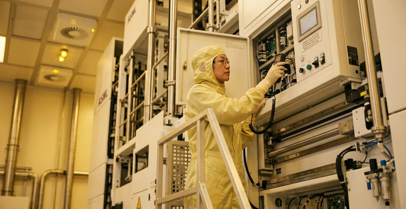
ASML occupies a position no other WFE player can claim: it is the only company in the world that manufactures EUV lithography machines. Chris Miller, professor at Tufts University’s Fletcher School, described it bluntly in an interview with CNBC: “ASML has a monopoly on the fabrication of EUV lithography machines.” For advanced nodes below roughly 7nm, there is no viable technological alternative.
$123 billion
Projected WFE segment sales for 2026, per SEMI’s forecast, driven by advanced logic and AI-linked memory demand.
That monopoly creates a dependency of a fundamentally different nature than anything in deposition or process control. TSMC, Samsung and Intel alone represented close to 84% of ASML’s revenue in 2021, according to the same CNBC reporting — a concentration that shows how tightly the leading edge is bound to a single supplier. EUV systems are also the most expensive single tools in a fab, and they are geopolitically sensitive: export controls restrict EUV shipments to China, making ASML a strategic asset well beyond commercial considerations.
The key point for any comparison: ASML does not compete with Applied Materials or KLA. Lithography is its exclusive domain. Any ranking that pits the three companies head-to-head on revenue or “leadership” compares apples to oranges — ASML’s strategic weight comes from irreplaceability, not breadth.
Applied Materials: breadth across deposition and etch
Applied Materials plays the opposite game. Where ASML is deep in one segment, Applied Materials is the broadest supplier in front-end processing, with leadership positions in deposition (CVD and PVD) and etch — the steps that actually build the chip’s material layers. Platforms like Endura (PVD), Centura (CVD) and Sym3 etch are workhorses across the process flow of any 300mm fab.
The operational footprint is telling. In a typical advanced fab, Endura systems deposit the conductive metal layers, Centura systems deposit insulating dielectrics, and Sym3 systems etch the patterns defined upstream by ASML lithography. Applied Materials tools therefore appear at multiple sequential stages of the same process flow — a breadth neither ASML nor KLA matches.
But breadth is not monopoly. Unlike ASML in EUV, Applied Materials shares its core segments with significant competitors, notably Tokyo Electron and Lam Research. For fab operations, that competitive landscape changes the negotiation dynamic: deposition and etch capacity can be sourced, benchmarked and renegotiated across multiple vendors, which gives procurement teams leverage they simply do not have on EUV lithography.
Where does KLA’s process control fit in the value chain?
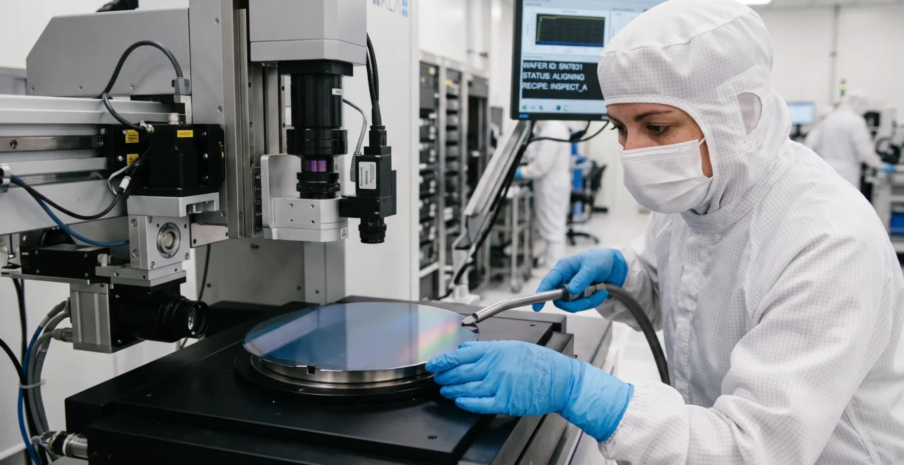
KLA’s tools do not build wafers — and that is precisely why they are indispensable. Inspection and metrology systems detect defects and measure critical dimensions at every process step. A Surfscan tool catching sub-micron contamination after a deposition step, or an e-beam inspection system resolving defects invisible to optical methods, prevents a bad batch from contaminating everything downstream. Process control is quality assurance, not manufacturing — but without it, yield collapses and nothing moves forward.
KLA’s own investor communications confirm the strength of its position: the company states that its leadership in process control is validated by recently published market share results, a claim made in its fiscal 2025 third-quarter results release. As with ASML, the strategic weight comes from specialization — KLA dominates a segment where the alternatives are far weaker.
Why process control downtime blocks entire production lines : KLA equipment does not fabricate wafers, but it validates them at each critical step. Without inspection and metrology, no wafer can advance — creating an absolute bottleneck when these systems go down. This is a different failure mode from a deposition chamber outage, where parallel chambers can absorb the load. That is what makes spare parts availability for process control tools disproportionately strategic.
This is where the aftermarket dimension enters the picture — and where most comparative analyses stop short. When a metrology system blocks the line, the downtime cost is measured against every wafer waiting for validation. Fab operators routinely report that sourcing critical parts through traditional OEM channels can stretch to several weeks depending on part criticality and OEM stock. That gap between “weeks” and “the line is down” is exactly why specialized aftermarket partners — such as Eumetrys Spare Parts, which focuses on qualifying KLA-compatible spare parts with faster delivery — have emerged as an operational lever, not just a cost lever.
How do their market positions compare?
On paper, the three companies differ in scale and focus. Publicly available financial reporting shows ASML and Applied Materials operating at a substantially larger revenue scale than KLA, whose business is concentrated in process control and adjacent segments. Direct, precisely quantified market share figures per segment vary across analyst sources and are not consistently published — which is itself worth knowing before citing any single number in a board presentation.
What the verified data does support is a comparative reading of focus rather than rank:
| Criterion | ASML | Applied Materials | KLA |
|---|---|---|---|
| Core segment | Lithography (DUV/EUV) | Deposition, etch, broad front-end | Process control (inspection, metrology) |
| Competitive position | Only EUV manufacturer worldwide (per expert commentary cited by CNBC) | Leader among several strong competitors (incl. Tokyo Electron, Lam Research) | Leadership confirmed by published market share results (company reporting) |
| Fab dependency profile | Absolute for advanced nodes | High volume, negotiable across vendors | Critical bottleneck when unavailable |
| Lifecycle stakes | Very high per-tool investment, export-controlled | Large installed base, multi-vendor sourcing | Spare parts availability drives line uptime |
The paradox worth remembering: revenue scale does not equal strategic weight. ASML’s monopoly position creates a dependency that its raw revenue figure understates, and KLA’s smaller footprint in dollars does not diminish the operational criticality of its tools — a single blocked metrology step can idle far more value than the tool itself represents.
- Scale is misleading: the biggest by revenue is not the most irreplaceable on the line.
- Each company dominates a distinct segment — lithography, deposition/etch, process control — rather than competing head-to-head.
- Precise per-segment market shares vary by analyst source; treat single figures with caution.
What operational factors matter beyond equipment performance?
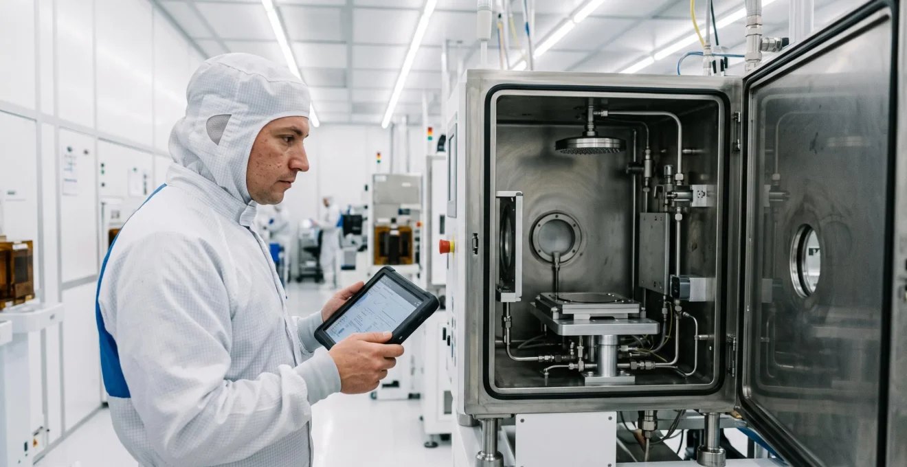
The purchase price is only the visible part of the cost. Total Cost of Ownership includes maintenance contracts, spare parts, uptime guarantees and the real cost of unplanned downtime — figures that dwarf the capital line item over a tool’s life. Equipment purchased once is supported for a decade or more, and the terms negotiated at procurement do not cover everything that happens between day one and decommissioning.
OEM spare parts lead times impact critical uptime : sourcing parts through traditional OEM channels routinely takes multiple weeks — fab operators commonly report lead times in the range of 3 to 6 weeks for non-stocked critical parts. When a process control tool blocks an entire line during that window, the production cost of waiting can exceed the part cost by orders of magnitude. This asymmetry is precisely what drives fabs to diversify their sourcing.
Managing the inevitable triple dependency — ASML, Applied Materials, KLA in the same fab — therefore extends well into lifecycle strategy: standardizing maintenance procedures across vendors, cross-training engineering teams, and, critically, diversifying spare parts sourcing beyond single OEM channels. For KLA-critical equipment in particular, working with specialized aftermarket suppliers like Eumetrys Spare Parts can compress sourcing from weeks to days on qualified parts, directly protecting uptime targets. For teams managing the maintenance side of heavy industrial equipment more broadly, understanding the scope of onsite machining offers a useful parallel on how service responsiveness reduces downtime exposure.
When downtime risk on a critical tool escalates into a production or safety question, the same logic applies across industries — the cost of prevention is trivial next to the cost of an unmanaged failure.
The practical takeaway reframes the original question. KLA, ASML and Applied Materials are not three options to weigh — they are three structural dependencies to manage. Every capital negotiation, maintenance contract and spare parts strategy should be built on that premise. The fabs that perform best are not the ones that “picked a winner”; they are the ones that manage multi-vendor risk deliberately, from procurement through the entire equipment lifecycle, including the aftermarket channels most comparisons never mention.